Moving to Altium Designer from PADS Layout and OrCAD capture
Contents
- Getting Started - Transferring Your PADS Layout Designs
- Layer Mapping for PADS PCB ASCII Files
- Using the Import Wizard for OrCAD Capture Designs
- OrCAD Capture 10.x *.DSN Files and the Unrecognized Project File Version Error
- Sheet Structure in OrCAD Capture's Project Manager
- Defining Net Connectivity
- The Schematic Symbol is the Part
- Design Rules Scoping
- Altium Designer Libraries
- See Also
Getting Started - Transferring Your PADS Layout Designs
Translating complete PADS Layout® designs, including PCB files and library files can all be handled by Altium Designer's Import Wizard. The Import Wizard removes much of the headache normally found with design translation by analyzing your files and offering many defaults and suggested settings for project structure, layer mapping, PCB footprint naming, and more. Complete flexibility is found in all pages of the Wizard, giving you as little or as much control as you would like over the file translation settings, before committing to the actual translation process.
Using the Import Wizard for PADS Layout Files
The Import Wizard can be launched from the Altium Designer File menu. Click on this menu command to invoke the wizard. Right-click pop-up menus are available for further control over the translation process through each page of the wizard.
Files in the Import Wizard translate as follows:
- PADS ASCII PCB Layout (*.ASC) files translate to Altium Designer PCB files (*.PcbDoc)
- PADS ASCII PCB Library files translate as follows translate into Altium Designer PCB library files (*.PcbLib)
- These files will be grouped into an Altium Designer PCB project (*.PrjPCB) that is automatically created.

Use the Layer Mapping Options from the Edit Mapping button in the Import Wizard to associate PADS PCB layers to Altium Designer layers.
Layer Mapping for PADS PCB ASCII Files
All used PADS PCB layers must be mapped to an Altium Designer layer prior to import when using the Import Wizard. There are additional options provided to control the automatic creation of design rules, missing vias and keep-out conversions as well.
It should be noted about how the layers are mapped on import for PCB designs. Layer Mapping is simply a mapping between the names of the PADS PCB layers and Altium Designer PCB layers. Of course you can change as many mappings as you want as only suggested default mappings are given. This mapping is used by the Import Wizard to build the layer mapping for each PCB that can then be individually customized. The rationale here is that should you wish to import ten PCB designs and you want to map the layer Assembly 1 to Mechanical Layer 1, you would not have to customize each of the ten PCB designs in order to get the right layer mapping.
The advantage to importing in this manner is that batch management of layer mapping can save a lot of time when importing multiple designs. In this instance, the default layer mapping will be saved to your Preferences. The disadvantage to using this is that Default Layer Mapping is not always intelligent with differing structures in designs, and so some manual changes may be needed afterwards. You'll need to decide what is best for your situation.
Turning the Override Pad Inner Value option on means that imported pads will have their sizes on the midlayers set to the largest size found.
Using the Import Wizard for OrCAD Capture Designs
If you are using OrCAD Capture™ Schematic files in combination with your PADS Layout PCB designs, you can still use the Import Wizard. Files in the Import Wizard translate as follows:
- OrCAD Capture (*.DSN) files translate to Altium Designer schematic files. Each page within a .DSN file will be imported as a single Altium Designer schematic file (*.SchDoc). Design caches within a .DSN file will be imported as a schematic library (*.SchLib). Design hierarchy is maintained, including complex hierarchy
- These files will be grouped into an Altium Designer PCB project (*.PrjPCB) that is automatically created.
OrCAD library files translate as follows: - OrCAD OLB (schematic library) files will be translated into Altium Designer schematic library files (*.SchLib)
- Translated OrCAD libraries are automatically grouped into one PCB project.
OrCAD Capture 10.x *.DSN Files and the Unrecognized Project File Version Error
The file format of *.DSN files changed in OrCAD Capture 10.x. *.DSN files saved normally in OrCAD Capture 10.x and higher may be incompatible with Altium Designer releases earlier than Summer 09 (and also, it may be added, with releases of OrCAD Capture earlier than 10.x). Attempting to import a 10.x *.DSN file into Altium Designer Winter 09 or earlier may give you an Unrecognized Project File Version error.
If you encounter this problem, there are two ways you can fix it:
- Upgrade to Altium Designer Summer 09 (or later), which recognizes the OrCAD Capture 10.x file format.
- Resave the *.DSN file in OrCAD Capture 10.x in the older format. To do this, start OrCAD Capture 10.x, and make sure the DSN is selected in the project panel. Run File » Save As. You will see a small check box saying Remove Pin Name and Number Movement. This check box will appear if pin name and numbers have been moved in 10.x. Check it and save the DSN file. The DSN file can now be imported into Altium Designer Winter 09 and earlier.
Sheet Structure in OrCAD Capture's Project Manager
Like Altium Designer, Capture supports flat and hierarchical designs. Both use a block-like symbol to define sheet-to-sheet structure in a hierarchical design, called a Sheet Symbol in Altium Designer, and a Hierarchical Block in Capture. In both, the symbol references the lower level schematic. In Altium Designer this is simply another schematic sheet; in Capture it can be more complex.
Capture has another layer of design partitioning that affects hierarchy. In Capture there is a schematic, which present as a folder icon in Capture's Project Manager, and there are pages, which present as a schematic sheet icon. Each Capture schematic can be made up of one or more pages. The Capture hierarchical block points to the schematic below, which means the block can actually reference circuitry divided over multiple pages.
Typically a flat Capture design is one schematic (folder), with the design being drawn on as many pages as required in that schematic (folder). For a hierarchical design, the hierarchical block symbol (or part with an attached schematic sheet or model) is the mechanism used to partition the major functional regions of a design.
For a simple hierarchy, each hierarchical block, or part with an attached schematic folder, or VHDL model, represents a unique design module. The Hierarchy tab in OrCAD Capture's Project Manager displays a simple hierarchical design as a tree of schematic pages. The schematic folder or VHDL entity at the top of a hierarchy, which directly or indirectly refers to all other modules in the design, is called the root module. In the OrCAD Project Manager's File tab, the root module has a backslash on its folder icon, shown below. The root module folder, as well as any other module folder, can contain as many schematic pages or VHDL models as required.
On the left is the structure of an example CPU_Design project as it would appear in OrCAD Capture.
On the right is the same project CPU Design after import in the Projects panel of Altium Designer.
Defining Net Connectivity
In OrCAD Capture, net connectivity is made using net aliases, off-page connectors, hierarchical blocks and hierarchical ports, and globals. Nets between schematic pages within a single schematic folder are connected through the off-page connectors while the hierarchical blocks and ports connect the nets between the schematic folders. Globals are used to connect power/ground nets throughout the design.
Altium Designer uses a similar set of net identifiers to create net connectivity. Within a schematic sheet you can use Wires and Net Labels. Between schematic sheets, nets in a flat design are typically connected using Ports, but Off-Sheet Connectors are also available. Nets in a hierarchical design are connected from a Port on the lower sheet to a Sheet Entry of the same name, in the sheet symbol that represents the lower sheet. Power/ground nets are connected using Power Ports.
The Schematic Symbol is the Part
As an expert PADS Layout user, you'll know that parts form the basic building blocks of design in PADS Layout. Parts are defined as having a part type, a logic family, number of pins, number of gates, and signal pins. The term component is only used when the part becomes placed as a physical object in the PCB layout design.
In PADS Layout (PCB), a part can represent one or more physical components. Parts in PCB designs usually correspond to physical objects: gates, chips, connectors, objects that come in packages of one of more parts. Multiple-part packages are physical objects that are comprised of one or more parts.
In OrCAD's Capture, a part is a logical entity that is described graphically by a symbol, pins and various properties. As parts are placed in a schematic design, Capture maintains the identity of the part for back annotation, net listing, bills of materials, and so forth. At the very minimum, a part requires a part name, a part reference prefix, and a name of a PCB footprint.
These two definitions that use the same term depending on the context of design may initially cause some confusion in the new environment which uses the term component. But it is not unlike how things work in Altium Designer except that the schematic symbol is effectively the part for all phases of design, and not just the PCB Layout portion of it.
In Altium Designer, the logical symbol is assumed to be the essential starting point of a component. It can be initially defined at minimum as a name in a schematic library to which pins and any graphical symbols or alternative display options needed for implementation may be added. This flexibility allows a component to be represented in different ways during the design and capture process. This may not only be as a logical symbol on the schematic, but also be a footprint on the PCB or even as a SPICE definition for simulation.
Design Rules Scoping
It may arise that a design object is covered by more than one rule with the same scope. In this instance, a contention exists. All contentions are resolved by the priority setting. The system goes through the rules from highest to lowest priority and picks the first one who's scope expression (s) matches the object(s) being checked.
Rules Scope - the extent of a rule's application - replaces the Rules Hierarchy from PADS Layout. A scope is effectively a query that you build to define all the member objects that are governed by that rule, giving you full control.
For the sake of a baseline comparison, let's review the Rules Hierarchy of PADS Layout. These rules rely on a pre-defined list format where higher numbers on the list have precedence over those that are lower:
- Default
- Class
- Net
- Group
- Pin Pair
- Decal/Component
In the PADS Layout rules schema, Default rules are considered level 1 and are the lowest while Decal and Component rules represent the highest. Conditional layer rules can be applied for an additional level of precedence. For example, a Default with a conditional layer rule would be higher in the precedence hierarchy than a simple Default rule.
In Altium Designer, scoping allows you to decide exactly what a rule's precedence will be and how it will be applied to target objects through a query. You can even define multiple rules of the same type, but each targeting different objects. Queries are easily accessed for any rule. Advanced (Query) options are also available to help you write your own, more complex queries.
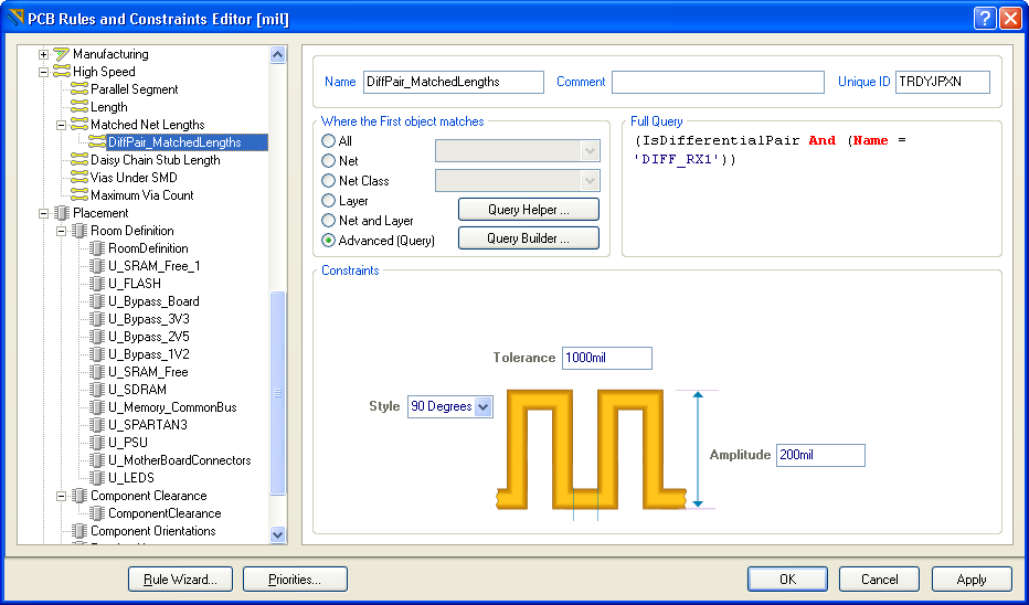
Double-clicking on any rule while in the PCB Rules and Constraint Editor dialog will bring up the specific query for that rule in the right pane.
All default design rules have a scope (Full Query) of ALL, meaning that they apply to the whole board. In addition to scoping, there is also a user-defined priority setting. The combination of rule scoping and priority is very powerful and gives an unprecedented level of control that allows you to precisely target the design rules for your board.
Altium Designer Libraries
An integrated library in Altium Designer is one where the source symbol, footprint, and all other information (e.g. SPICE and other model files) are compiled into a single file. During compilation checks are made to see how relationships are defined, to validate the relationship between the models and the symbols and to bundle them into a single integrated library. This file can not be directly edited after compilation, offering portability and security.
All of Altium Designer's 70,000+ components are supplied in integrated libraries, from which the source libraries can be extracted at any time if required.
| PADS Object | Altium Designer Object | Comments |
|---|---|---|
| Decal | Footprint | Graphical representation of the shape defined for the component to mount onto the PCB. This is 2-dimensional representation only, and can be quite different from the actual component itself |
| Part | Part/Component | The term Part is used only as part of the design capture (schematic) process in Altium Designer. Once placed as a footprint into a PCB file, it is given a designator and value (comment) and becomes a component. |
| Lines | Lines | Primitive object used for graphical information. |
| CAE Decal | Schematic symbol | The graphical representation of a schematic part, such as a NOR gate. |
A table of the more commonly-used PADS Library terms and their closest respective Altium Designer equivalents.
See Also
Below are references to other articles and tutorials in the Altium Designer Documentation Library that talk more about the conceptual information as well as walking you through specific tasks. Remember, you can also browse through the Help contents, and use F1 and What's This at any time in a dialog for more details.
For more PCB project options, refer to the tutorial, Getting Started with PCB Design.
For more FPGA project options, refer to the tutorial, Tutorial - Getting Started with FPGA Design.
For a tutorial that steps you through all the basics of creating components, read Creating Library Components Tutorial.
For an overview of Altium Designer's FPGA design, development and debugging capabilities, read Soft Design.