Embedded Board Array
Contents
Parent page: Objects
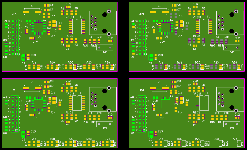
2 x 2 board array references a single PCB design
Summary
An embedded board array is a primitive design object. It allows you to create a PCB panel (representing the physical board that the PCB is to be manufactured from) as part of your PCB design project. This is also known as panelization . You can use this panel to hold an array of PCBs on using the embedded board array command. This command links the panel to the original PCB design files, stepping it out the specified number of times. You cannot edit the PCBs directly from the board array, only through their original files.
Multiple embedded board arrays can be placed and each can reference a different PCB file. By spacing out the boards in each array and then overlaying, rotating and flipping the different embedded arrays, any panelization arrangement can be created. This can be used to reduce manufacturing costs by maximizing the number of PCBs per panel of PCB material.
Availability
Embedded Board Arrays are available for placement in the PCB Editor only, by selecting Place » Embedded Board Array from the main menus.
Placement
- After launching the command, the cursor will change to a crosshair and you will enter embedded board array placement mode. The location of the crosshair decides the lower-left corner of the board array.
- Position this corner of the array at the required location and click or press Enter to place.
- Continue placing further embedded board arrays, or right-click or press Esc to exit placement mode.
The embedded board array object can be rotated or flipped while in placement mode:
- press the Spacebar to rotate the embedded board array. Rotation is anti-clockwise and in steps of 90°
- press the L key to flip the embedded board array to the other side of the board.
Non-Graphical Editing...
The following methods of non-graphical editing are available:
...via an Associated Properties Dialog
This method of editing uses the following dialog to modify the properties of an embedded board array object:
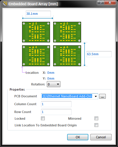
This dialog feature a units toggle control in the top-left corner that will change the units of measurement currently used in the dialog between metric and imperial [shortcut: CTRL + Q ]. The current unit of measurement is displayed in the dialog title area.
The Embedded Board Array dialog can be accessed prior to entering placement mode, from the PCB Editor - Defaults page of the Preferences dialog (Tools » Preferences). This allows you to change the default properties for the embedded board array object, which will be applied when placing subsequent embedded board arrays.
During placement, the Embedded Board Array dialog can be accessed by pressing the TAB key.
After placement, the Embedded Board Array dialog can be accessed in the following ways:
- double-clicking on the placed embedded board array object
- right-clicking the embedded board array object and selecting Properties from the pop-up menu
- selecting the Edit » Change command, then clicking once over the placed embedded board array object.
...via an Inspector Panel
An Inspector panel enables the designer to interrogate and edit the properties of one or more design objects in the active document. Used in conjunction with appropriate filtering, the panel can be used to make changes to multiple objects of the same kind, from one convenient location.
...via a List Panel
A List panel allows the designer to display design objects from one or more documents in tabular format, enabling quick inspection and modification of object attributes. Used in conjunction with appropriate filtering, it enables the display of just those objects falling under the scope of the active filter – allowing the designer to target and edit multiple design objects with greater accuracy and efficiency.
Graphical Editing
This method of editing allows you to select a placed embedded board array object directly in the workspace and change its location or orientation, graphically.
When an embedded board array object is selected, it is distinguished by light gray background. The images illustrate this for both an un-referenced board array and a 2 x 2 array that references a single PCB design.
![]()
Un-referenced board array
A 2 x 2 array that references a single PCB design
Click anywhere within the boundary of the array and drag to reposition it. The array is automatically 'grabbed' by its lower-left corner. The embedded board array can be rotated or flipped while dragging:
- press the Spacebar to rotate the embedded board array. Rotation is anti-clockwise and in steps of 90°
- press the L key to flip the embedded board array to the other side of the board.
Notes
- The embedded board array(s) used to create a representation of the manufacturing panel should be placed on a separate PCB document within the existing or alternate PCB project. This document should be considered as the manufacturing 'hub' for other PCB documents that contain the actual designs.
- You can place additional objects to support panel manufacturing (for example free pads as tooling holes), but it is not advisable to place any other objects that would represent the actual physical design, within the same document as the embedded board array(s).
- As the embedded board array object references a PCB design file, rather than containing a pasted copy of it, the source PCB design may be modified at any time. Once the reference file is saved, refresh the view of the panel document in order to bring the panel up-to-date.
- Gerber, NC Drill, ODB++ and printed output can be generated from a panel of embedded board arrays.